


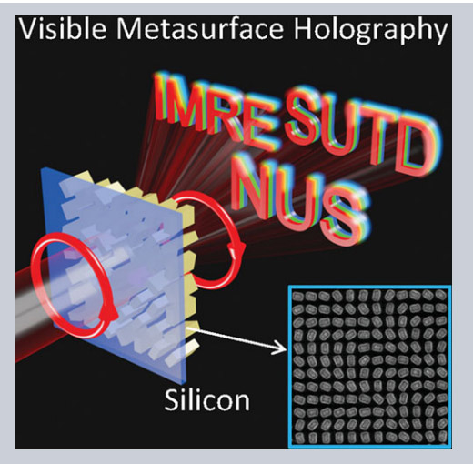
To date, hologram technology uses reflected light to form an image, which causes the image to be muddled up with the light source. Joel Yang and Dong Zhaogang from the A*STAR Institute of Materials Research and Engineering have however recently pioneered a hologram that uses transmitted instead of reflected light. Although this does not mean we can send videos to Obi-Wan Kenobi on our droid, the new hologram does work throughout the visible spectrum.
Using an array of silicon structures, the research team demonstrated the hologram of three flat images. Wavelengths ranging from red (680 nanometers) to blue (480 nanometers) were used and he images appeared in planes 50 microns apart for red with a higher spacing for the shorter wavelengths.
Holograms store large amounts of information in increasingly thin layers by recording three-dimensional images, and according to Yang, they can be tuned to any wavelength.
Silicon holograms are slightly thicker than the alternative of a mere hundredths of the thickness of a human hair achieved by metal deposited onto materials such as silicon. In the metal-based holograms, images are created by nanoscale patterns of metal that generate electromagnetic waves. These waves then travel at the metal–silicon interface and create a field called plasmonics.
The silicon counterparts, although thicker, have the advantage of being broadband, as opposed to metal-based holograms that can only operate in the red wavelengths. Blue wavelengths are absorbed by plasmonic holograms. Although silicon holograms have poor efficiency at only three per cent, Dong guesses this could easily be raised to nine percent. He notes that this can be achieved by not using amorphous silicon but optimizing the growth method used to grow polycrystalline silicon instead.
The hologram consists of an array of minute silicon skyscrapers, with footprints 190 nanometers by 100 nanometers and 370 nanometers tall. The tiny towers are not laid out in neat squares as a city grid is, but rather at varying angles.
The varied angles of the skyscrapers encodes information on to the circularly polarized light beam. The ‘Pancharatnam–Berry effect’ then alters the phase of the light transmitted by the skyscrapers. Yang notes that it is interesting that the hologram controls only the phase of the light by changing the alignment of the silicon nanostructures, while the same amplitude is observed everywhere. This has the effect of a lot of light being transmitted.
Study has been published in the Laser & Photonics Reviews.
Save
