


Carbon nanotubes (CNTs) have an amazing optical, electrical, mechanical and thermal characteristics. Some CNTs are semiconductors while others are conductors, scientists have been researching them for years with the objective of using them as future replacements for silicon.
There are however a number of challenges that remain to be solved before CNTs can be used on a big scale. These include finding production methods that will allow engineers to place them in specific locations on smooth substrates in such a way that it will lead to the formation of circuits around them. Current methods can’t be implemented commercially because they are imprecise, costly and slow.
CNTs are extremely small and, as their name indicates, their size is measured in nanometers. A typical CNT’s diameter is 100,000 times smaller than the thickness of a human hair. This is too small to be seen and studied using a conventional optical microscope. Rather than using the traditional method of relying on the chemical properties of CNTs to bind marker molecules Prof. Yaish, and graduate students Michael Shlafman and Gilad Zeevi of Technion’s Viterbi Faculty of Electrical Engineering and the Zisapel Nanoelectronics Center, approached the problem from a totally different angle. Yaish explains that on a flat and uniform surface, CNT is both a chemical and physical defect, making it possible for it to serve as a seed for the nucleation and growth of nanocrystals. Although nanocrystals are small, they are optically visible.
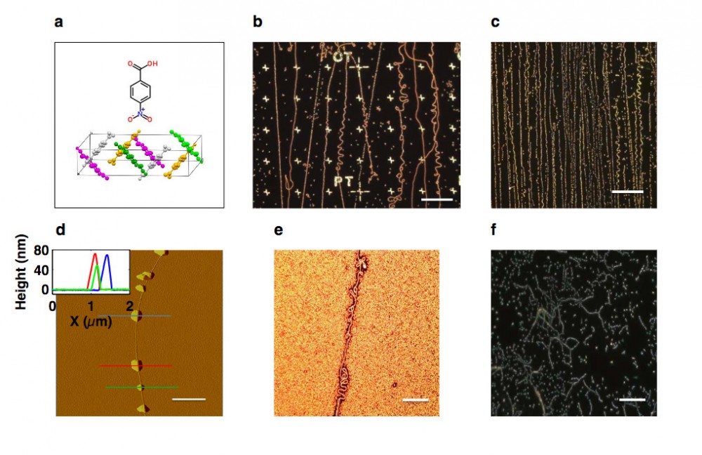
The CNTs are grown directly and then coated with the aid of the organic crystals. This makes it possible to see them under a microscope and use image identification software to find and produce a transistor. The CNTs can be removed completely after imaging, as they are not bound to the surface. This also means that electrical and mechanical properties of the CNT are preserved. The new method has the added benefit of making it possible to study the dynamic properties of CNTs, including resonance (vibration), the transition from softness to hardness and acceleration.
From manufacturing a single transistor, it’s a small step to move into producing a single chip (VLSI) and then an integrated circuit of miniaturized electronic components. Once this is perfected, the new devices are bound to be suitable as replacements for silicon electronics.
The goal is to integrate CNTs in an integrated circuit of miniaturized electronic components (mainly transistors) on a single chip (VLSI). Once the goal has been achieved, it paves the way for the integration of nano-electronics with silicon technologies. This could ultimately lead to molecular electronics replacing silicon chips as the building blocks of electronics.
The full study was published in Nature Communications journal.
Save
